2023, Articles, Cyberculture, Technologies
NRE Cost Optimization for Electronics: A Comprehensive Guide

Jun
NRE Cost Optimization for Electronics by Jacques Gascuel This article will be updated with any new information on the topic, and readers are encouraged to leave comments or contact the author with any suggestions or additions.
Summary
NRE cost optimization for electronics is a key factor for ensuring the profitability of electronic product development. NRE cost can be reduced by using different levers and tools, such as optimizing the V-cycle, the WBS, and the schedule, and using the TRL scale to assess the maturity of technologies. Freemindtronic is an example of a company that uses these techniques to optimize NRE cost for its electronic products with PCB, which are based on its patented technologies and offered under license and white label services.
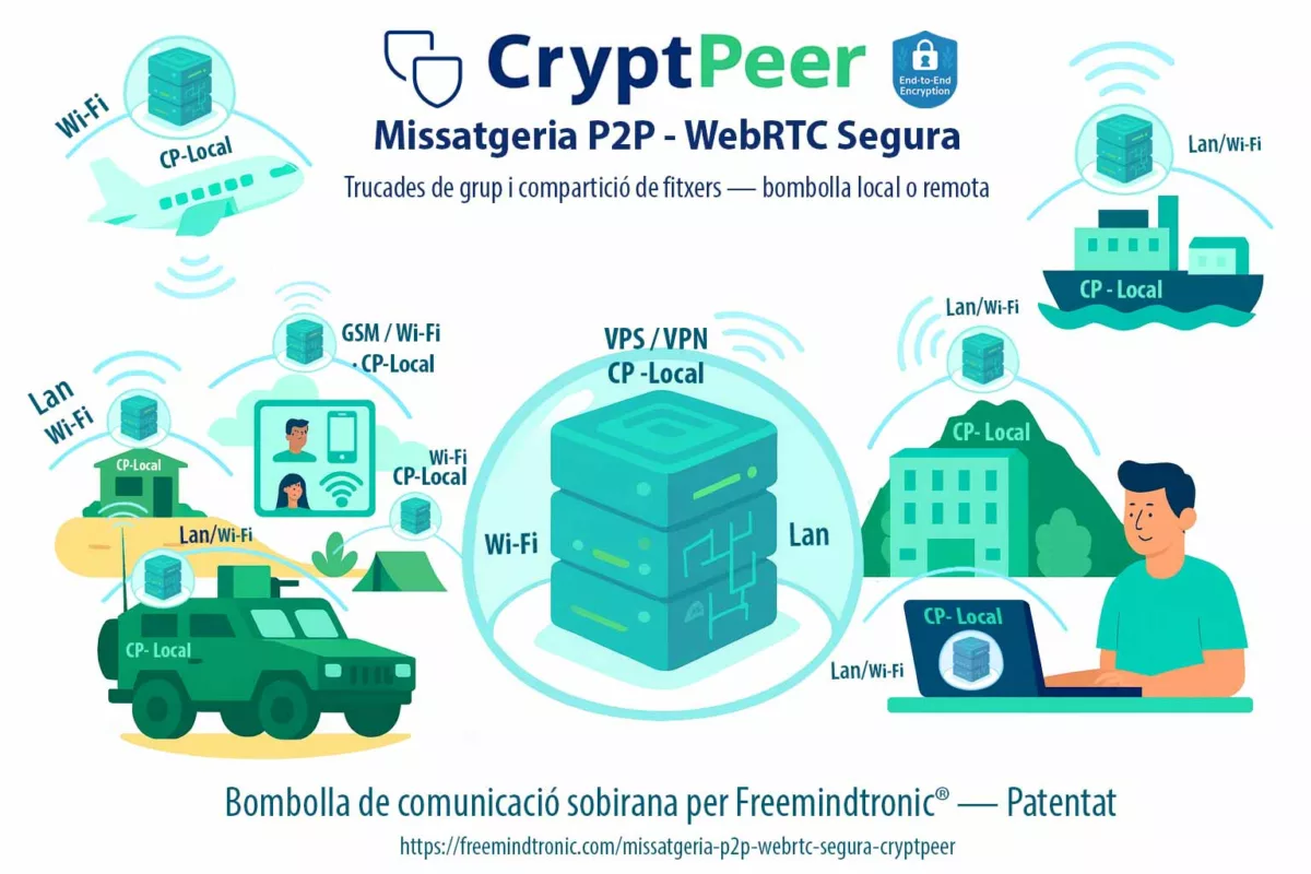
2025 CyptPeer Digital Security EviLink
Missatgeria P2P WebRTC segura — comunicació directa amb CryptPeer

2025 Cyberculture EviLink
P2P WebRTC Secure Messaging — CryptPeer Direct Communication End to End Encryption

2025 Cyberculture Cybersecurity Digital Security EviLink
CryptPeer messagerie P2P WebRTC : appels directs chiffrés de bout en bout

2026 Awards Cyberculture Digital Security Distinction Excellence EviOTP NFC HSM Technology EviPass EviPass NFC HSM technology EviPass Technology finalists PassCypher PassCypher
Quantum-Resistant Passwordless Manager — PassCypher finalist, Intersec Awards 2026 (FIDO-free, RAM-only)
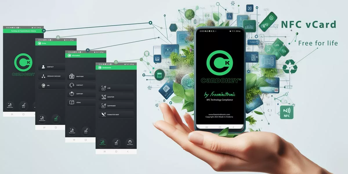
2024 Articles Cardokey EviSwap NFC NDEF Technology GreenTech Technical News
NFC vCard Cardokey: Revolutionizing Digital Networking

2024 Articles Cyberculture EviPass Password
Human Limitations in Strong Passwords Creation

2024 Articles Digital Security EviKey NFC HSM EviPass News SSH
Terrapin attack: How to Protect Yourself from this New Threat to SSH Security

2023 Articles Cyberculture EviCypher NFC HSM News Technologies
Telegram and the Information War in Ukraine
Discover our other articles on digital security
Efficient NRE Cost Optimization for Electronics
NRE Cost Optimization, in the field of electronic product development, plays a central role. This one-time cost, associated with designing, testing, and developing a new product, has a direct impact on the product’s unit cost and the profit margin. Therefore, estimating and optimizing NRE cost are essential for ensuring the project’s viability and profitability.
NRE cost depends on several factors, such as:
- The complexity and size of the product
- The quantity and frequency of the orders
- The technology, tools, and methods used for designing, manufacturing, and testing the product
- The software associated with the product
- The royalty fee paid to the technology provider
The complexity and size of the product can drive up the costs due to the increase in material and labor costs. On the other hand, larger and repeated orders can reduce the NRE cost per unit, as fixed costs are distributed over more units.
In this article, we will explain how to calculate NRE cost for electronic products with PCB (printed circuit boards), which are the core components of any electronic device. We will also present three main levers to reduce NRE cost for electronic products with PCB: optimizing the V-cycle, optimizing the WBS (work breakdown structure), and accelerating schedule. Finally, we will introduce the TRL scale (technology readiness level scale), a tool that can help you optimize NRE cost for electronic products with PCB by assessing and comparing the maturity of different technologies.
We will also show you how Freemindtronic, an Andorran company specialized in security and cybersecurity of computer systems and information systems, uses the TRL scale to optimize NRE cost for its electronic products with PCB. Freemindtronic also offers its technologies under license, including international patents, and provides white label product creation services.
How to Calculate NRE Cost for Electronic Products with PCB?
To optimize NRE cost for electronic products with PCB, you need to know how to calculate it. NRE cost can be divided into four main categories:
- Design cost: this includes the software tools for CAD (computer-aided design), licenses, salaries of designers, etc.
- Fabrication cost: this includes the materials, equipment, tools, personnel, etc. for manufacturing the electronic components and assembling them into a product.
- Test cost: this includes the measurement devices, test software, salaries of testers, etc. for verifying the functionality and quality of the product.
- Software cost: this includes the firmware, drivers, embedded systems, applications, extensions, etc. associated with the product.
- Royalty cost: this includes the fee paid to the technology provider for using their technology in the product.
To calculate NRE cost for electronic products with PCB, you need to estimate the time and resources required for each category. You can use historical data from previous projects or industry benchmarks as references. You can also use online calculators or software tools to help you estimate NRE cost.
In addition to these categories, you also need to consider the software associated with the PCB,
which ensure its functionality and interaction with the user or other systems. The software associated with the PCB include:
- Firmware: they are embedded in the PCB and control the behavior of the electronic components. They are usually written in low-level (assembler) or intermediate-level (C, C++, etc.) languages. They are specific to the product and must be adapted to the characteristics of the PCB and the electronic components.
- Drivers: they are installed on the computer or system that communicates with the PCB. They allow the system to recognize the PCB and transmit data between the PCB and the system. They are usually written in high-level (C#, Java, Python, etc.) languages. They must be compatible with the operating system and communication protocol used.
- Embedded systems: they are installed on the PCB or on another support (memory card, hard disk, etc.). They allow to manage the functions of the product and provide a user interface. They are usually written in high-level (C#, Java, Python, etc.) languages. They must be adapted to the capabilities of the PCB and the needs of the product.
- Applications: they are installed on the computer or system that communicates with the PCB. They allow the user to access the functionalities of the product and customize its settings. They are usually written in high-level (C#, Java, Python, Go, Type script, elvet etc.) languages. They must be ergonomic and intuitive for the user.
- Extensions: they are installed on the computer or system that communicates with the PCB. They allow to add functionalities to the product or connect it to other services or systems. They are usually written in high-level (html, type script, web RTC, Java, java script, etc.) languages. They must be secure and respect compatibility standards.
These software must be designed, developed and tested in parallel with the PCB, in order to guarantee their coherence and performance. They must also be updated regularly to correct any bugs or to bring improvements to the product.
Besides these categories, you also need to consider the tools required for manufacturing and testing the PCB, which depend on the characteristics of the PCB and the requirements of the product. The tools for manufacturing and testing the PCB include:
- Soldering machines: they allow to assemble electronic components on the PCB by soldering. There are different types of soldering machines, depending on the process used (wave soldering, reflow soldering, selective soldering, etc.).
- Insertion machines: they allow to insert electronic components through holes in the PCB. They are used for through-hole components, which are fixed by soldering on both sides of the PCB.
- Placement machines: they allow to place electronic components on the surface of the PCB. They are used for SMD (surface mount device) components, which are fixed by soldering on one side of the PCB.
- Cutting machines: they allow to cut the PCB according to the desired shape. They are used to separate the different parts of the PCB or to adjust the size of the PCB.
- Drilling machines: they allow to drill holes in the PCB to insert components or connectors. They are used to make connections between the different layers of the PCB or between the PCB and other elements.
- Engraving machines: they allow to engrave patterns or inscriptions on the PCB. They are used to identify the PCB or to add technical or aesthetic information to it. For example, you can engrave the serial number, the manufacturer name, or the logo of the product on the PCB.
- Measurement devices: they allow to verify the electrical and physical characteristics of the PCB. They include various devices such as multimeters, oscilloscopes, logic analyzers, insulation testers, etc. These devices allow you to measure the electrical and physical characteristics of the PCB, such as voltage, current, resistance, capacitance, frequency, etc.
- Test software: they allow to control the functionality of the PCB and electronic components. They include various software such as simulation software, fault injection software, functional analysis software, etc. These software allow you to test the behavior of the PCB and electronic components under different conditions and scenarios.
These tools must be chosen according to the type and complexity of the PCB, as well as the level of quality required for the product. They must also be calibrated and maintained regularly to ensure their reliability and accuracy.
To illustrate how to calculate NRE cost for electronic products with PCB, let’s take an example of a project that involves developing a new product based on a 4-layer PCB with 1000 components (800 SMD and 200 through-hole). The project duration is 12 months and requires two engineers (one for design and one for test) with a salary of $3000 per month each. The project also requires a CAD software license ($5000), a fabrication service ($5000), a test service ($5000), a software development service ($10 000), and a royalty fee (5% of sales).
The following table shows how to calculate NRE cost for this project:
| Item | Formula | Cost |
|---|---|---|
| Human resources | (3 000 + 2 000) x (1 + 0.5) x 2 x 12 | $90 000 |
| Software tools | – | $10 000 |
| Materials | – | $5 000 |
| Equipment | – | $15 000 |
| Software | – | $10 000 |
| Royalty fee | 0.05 x 200 000 | $10 000 |
| Total NRE cost | Sum of above items | $140 000 |
As you can see, NRE cost can be quite high for electronic products with PCB, especially if the product is complex or requires specific technologies or tools. Therefore, it is important to optimize NRE cost by using different levers and tools that can improve the efficiency and quality of the product development process.

Three Main Levers to Reduce NRE Cost for Electronic Products with PCB
To optimize NRE cost for electronic products with PCB, you need to know how to reduce it. NRE cost can be reduced by using different levers and tools that can improve the efficiency and quality of the product development process. In this section, we will present three main levers to reduce NRE cost for electronic products with PCB:
- Optimizing the V-cycle: this is to optimize the design process of the product, which follows a V-shaped model that consists of four main phases: definition, design, verification, and validation. Optimizing the V-cycle relies on the following sub-levers:
Defining clearly and precisely the customer needs and product specifications, which are translated into functional and technical requirements for the product. This helps to avoid ambiguity and misunderstanding, and to align the expectations of all stakeholders. Designing modular and scalable product, which allows reusing existing components or technologies and adapting easily to future changes or improvements. This helps to reduce the design cost and time, and to increase the flexibility and adaptability of the product. Making prototypes and mock-ups, which allow testing the product in real conditions and collecting customer feedback. This helps to validate the feasibility and functionality of the product, and to identify and correct any errors or defects before mass production. Planning rigorously and realistically the project, taking into account technical, financial, and temporal constraints, and anticipating possible contingencies. This helps to optimize the use of resources, to avoid delays and budget overruns, and to manage risks effectively. Monitoring and controlling regularly the project, using performance indicators and appropriate project management tools, which measure the progress of the project and identify deviations from the initial plan. This helps to ensure the quality and efficiency of the project execution, and to take corrective actions if needed. Validating systematically the product at each stage of the V-cycle, using appropriate methods and test criteria, which ensure compliance and quality of the product. This helps to verify that the product meets the customer needs and product specifications, and to obtain certification or approval from relevant authorities.
- Optimizing the WBS (work breakdown structure): this is to structure the project into sub-projects, tasks, and activities, which are hierarchized and detailed according to their level of complexity and dependence. Optimizing the WBS relies on the following sub-levers:
Decomposing logically and coherently the project, respecting the principle of sum of parts equal to whole, that is, each element of WBS must contribute to achieving global project. This helps to clarify the scope and objectives of the project, and to avoid duplication or omission of work. Defining clearly and precisely deliverables associated with each element of WBS, specifying expected features, responsibilities, deadlines, and costs. This helps to define the expected outcomes of each element of WBS, and to assign roles and responsibilities to each actor of the project. Assigning resources needed for each element of WBS, taking into account skills, availability, and costs of human, material, and financial resources. This helps to allocate resources efficiently and effectively to each element of WBS, and to optimize the cost and quality of the project. Coordinating and communicating among different actors of project, using collaborative tools and agile methods, which promote information exchange and problem solving. This helps to ensure the coherence and consistency of the project, and to foster the collaboration and innovation among different actors.
- Accelerating schedule: this is to reducethe total duration of project by optimizing use of available resources and minimizing idle times. Accelerating schedule relies on following sub-levers:Reducing duration of critical tasks that have direct impact on end date of project. For this, we can use techniques such as crashing (increasing resources assigned to a task) or fast-tracking (performing tasks in parallel instead of sequentially). This helps to shorten the critical path of the project, which determines the minimum time required for completing the project. Increasing parallelism of non-critical tasks that do not affect the end date of project, but can reduce the total duration of project. For this, we can use techniques such as overlapping (starting a task before the previous one is completed) or splitting (dividing a task into smaller subtasks that can be performed in parallel). This helps to increase the concurrency of tasks in the project, which reduces idle times and improves resource utilization. Eliminating or minimizing slack time of tasks that is the difference between the earliest and latest start or finish times of a task. For this, we can use techniques such as resource leveling (balancing the demand and supply of resources over the project duration) or resource smoothing (adjusting the resource allocation to reduce peaks and valleys in resource usage). This helps to optimize the slack time of tasks, which can be used to absorb uncertainties or delays, or to improve quality or performance.
These levers and tools can help you optimize NRE cost for electronic products with PCB by reducing errors, delays, and budget overruns by improving the quality and efficiency of the product development process. They can also increase customer satisfaction and confidence by demonstrating the compliance and quality of the product at each stage of development.
How to Use the TRL Scale to Optimize NRE Cost for Electronic Products with PCB?
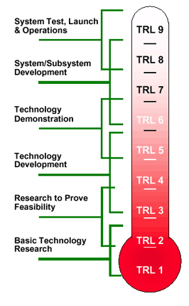
Another tool that can help you optimize NRE cost for electronic products with PCB is the TRL scale, or technology readiness level scale. The TRL scale is a tool for measuring or indicating the maturity of a technology. It was originally developed by NASA in the 1990s as a means to manage the technological risk of its programs. The TRL scale can help you optimize NRE cost for electronic products with PCB by providing a common language and framework for assessing and comparing the maturity of different technologies in the context of a specific application, implementation, and operational environment. The TRL scale also helps you identify gaps and risks in your technology development process, and plan appropriate actions and resources to address them.
The TRL scale ranges from 1 to 9, with 9 being ready for commercialization. The TRL scale describes the performance history of a given system, subsystem, or component relative to a set of levels that correspond to different stages of development.
The following table summarizes the main characteristics and criteria of each TRL level:
The following table summarizes the main characteristics and criteria of each TRL level:
| TRL | Definition | Description | Criteria |
|---|---|---|---|
| 1 | Basic principles observed | Scientific research begins and results are translated into future research and development | Publication or report of basic principles |
| 2 | Technology concept formulated | Basic principles are applied to practical applications and experimental proof of concept is obtained | Publication or report of applied research |
| 3 | Analytical and experimental critical function and/or characteristic proof-of-concept | Active research and design begin and proof-of-concept model is constructed | Analytical studies and laboratory tests |
| 4 | Component/subsystem validation in laboratory environment | Component pieces are tested with each other in a simulated environment | Component integration and testing |
| 5 | Component/subsystem validation in relevant environment | Breadboard technology is tested in a realistic environment with simulated interfaces | System-level testing in relevant environment |
| 6 | System/subsystem model or prototype demonstration in a relevant environment | Fully functional prototype or representational model is demonstrated in a realistic environment with actual interfaces | System-level testing in relevant environment |
| 7 | System prototype demonstration in an operational environment | Working model or prototype is demonstrated in an extreme environment with all interfaces | System-level testing in operational environment |
| 8 | Actual system completed and qualified through test and demonstration | Technology has been tested and “flight qualified” and is ready for implementation into an existing technology or technology system | System-level testing in operational environment |
| 9 | Actual system proven through successful mission operations | Technology has been “flight proven” during a successful mission and meets all performance requirements | System-level testing in operational environment |
What are the Benefits of Using the TRL Scale for Freemindtronic?
By using the TRL scale, Freemindtronic was able to achieve the following benefits:
- Providing a common language and framework for assessing and comparing the maturity of its technology with other technologies on the market.
- Identifying gaps and risks in its technology development process and planning appropriate actions and resources to address them.
- Reducing errors, delays, and budget overruns by improving the quality and efficiency of its product development process.
- Increasing customer satisfaction and confidence by demonstrating the compliance and quality of its product at each stage of development.
Freemindtronic also offers its technologies under license, including international patents, and provides white label product creation services. This allows its customers to protect their products and services created in their brand and embedding Freemindtronic’s technologies. In addition, they benefit from territorial protection in terms of international intellectual property. Freemindtronic also offers the possibility of negotiating an NRE royalty with its customers, depending on the added value of its technology and market conditions. Moreover, Freemindtronic has designed a mutualized offer of its NRE costs, distributed among all its customers under licenses. This has the effect of reducing the royalty cost attached to the NRE. This also has the effect of making affordable access to the different licenses, especially patented ones, which produce a low impact on the products marketed.
Freemindtronic guarantees an industrial quality of its products,
manufactured with industrial grade electronic components. It also ensures a complete traceability of the manufacture of its offline products and end-to-end cybersecurity from HSMs, from design to end user.
Conclusion and Contact Information
We hope that this article has given you some useful insights on how to optimize NRE cost for electronic products with PCB by using different levers and tools. We also hope that you have learned how to use the TRL scale to optimize NRE cost for electronic products with PCB by assessing and comparing the maturity of different technologies.
We also showed you how Freemindtronic, an Andorran company specialized in security and cybersecurity of computer systems and information systems, uses the TRL scale to optimize NRE cost for its electronic products with PCB. Freemindtronic also offers its technologies under license, including international patents, and provides white label product creation services.
If you have any questions or comments, please feel free to contact us. We will be happy to assist you with your project.
Thank you for your attention.